Fabrication of Silica Based Optical Waveguides Using Helicon Based Plasma Etching
and Deposition
ANDREW PERRY, ANTOINE DURANDET and ROD BOSWELL
Plasma Research Laboratory, R.S.Phys.S.E., ANU, Canberra ACT 0200
The challenge involved in the fabrication of silica planar buried channel waveguides
for integrated optics applications lies into the processing (deposition and etching)
of SiO2. Deposition of thick layers (up to 10 m) at low temperature (80 C) to allow the integration of active devices (detectors and diodes), has been achieved.
We successfully control the refractive index (with or without doping of the films),
the microstructure and the birefringence. We present the fabrication steps and their technological diffuculties, insisting on the underlying physics, and the performance
of some devices.
1. INTRODUCTION
The capability of integrating active devices with buried channel waveguides (BCW)
depends on the possibility of manufacturing low loss BCW at very low temperature.
Using plasma assisted deposition of doped silica it is possible to manufacture low
loss BCW, as already reported by many authors (1, 2, 3, 4). Nevertheless, although the deposition
process is done at low temperature, low-losses are only achieved after thermal annealing
at high temperature, above 500 C and in general towards 1000 C. The best results reported so far without thermal annealing are obtained at a processing
temperature of about 300 C (5, 6). Using the helicon plasma reactor (7) for deposition and etching of the
layers, we were able to perform all the fabrication steps at very-low temperature,
below 100 C. Furthermore, thanks to the flexibility of the helicon plasma source, it is possible
to control the energy of the ion bombardement impinging the surface during the deposition
independently of the plasma generation, allowing excellent control over the structure of the deposited material (8). The refractive index is controlled by fluorine
doping (5, 6), thus avoiding the use of poisonous gas such as germane or phosphine
used in conventional PECVD techniques. We fabricated single mode BCW (at 1.3 m and
1.55 m), with a square core of 5 m and n = (nco - ncl)/nco suitable for matching to optical fibre.
2. FABRICATION PROCEDURE
Standard 100 mm diameter silicon wafers (p type, orientation 100) were used as a substrate,
and did not receive any special cleaning. The deposition of silicon dioxide was achieved
using a helicon plasma reactor (8), by dissociation of a mixture of silane and oxygen. Thanks to the high efficiency of the helicon source, the deposition of
good quality SiO2 is achieved using pure oxygen, while most common PECVD systems operate from N2O. Thus, no nitrogen was introduced in the gas phase. The control of the refractive
index can be achieved by changing the ratio of oxygen to silane (7), or by doping
the layers with fluorine. This second technique is preferred, as it is very reproducible
and allows a very accurate control of the refractive indexes. We introduced a very
small amount of CF4, the silane flow and the oxygen flow being kept constant
at 12 sccm and 96 sccm respectively.
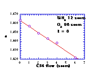
FIG.1: Evolution of the refractive index with the CF4 flow
The refractive indexes were measured using a prism coupler at 0.6328 m. The evolution
of the refractive index with the CF4 flow is given in Fig.1. The mechanism by which the refractive index changes with
the CF4 flow has already been reported elsewhere (6). Furthermore, the film is submitted
to an ion bombardment during deposition. The ions are extracted from the plasma by
applying a separate rf bias on the substrate, so that the energy of the ion bombardment
is maintained at 300 eV for all experiments. This value of the ion energy gives good
quality material (density and defects), and allows a good step coverage of the core
during cladding avoiding the formation of voids around the core. We have already
reported the effect of the ion energy on the quality of the deposited materials, justifying
the choice of 300 eV (8). The substrate is clamped on a water cooled holder, and
helium is circulating in the gap to ensure a good thermal contact. It has been verified,
using chemical sensors stuck on the back of the substrate, that, under these conditions,
the temperature of the wafer remains below 100 C. This value has also been confirmed by IR interferometry in a similar deposition
system.
A 7 m thick buffer layer is first deposited with 1.5 sccm of CF4 in the gas phase to give a refractive index of ncl = 1.451. The CF4 flow is then switched off to deposit the core layer (nco = 1.462). The deposition rate is about 100nm/min for both layers. After deposition
and lithography of a 150 nm thick Cr mask, the core layer is then plasma etched,
in a helicon plasma reactor identical to the one used for deposition, using CF4 chemistry. After removing the Cr mask (wet chemistry), the sample is cladd, in conditions
identical to those for the deposition of the buffer layer. The sample was not annealed.
For this BCW n = 0.007. Fig. 2 shows a cross-section of the BCW; thanks to the ion bombardment, the square core of the BCW is perfectly buried in the cladding
layer. The triangular feature at the top of the BCW is typical of the deposition
under ion bombardement, and due to the sputtering of the growing film.
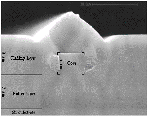
Fig.2: EM cross-section of a BCW fabricated with 300eV
3. IMPORTANCE OF THE ION BOMBARDMENT
An important feature of the helicon reactor is that it allows independant control
of the plasma generation and of the interaction of the plasma and the surface to
be processed, through independent biasing of the substrate. The energy of the ion
bombardement can thus be chosen. As already demonstrated (8), the energy of the ions impinging on the surface during the deposition influence all the aspects of the quality of
the films (structure,defects, stress, refractive index and porosity). Fig. 3 shows
an SEM cross-section of a BCW fabricated under similar conditions as the one presented earlier, but with very low energy of the ion bombardment (about 30 eV); the cross-section
clearly reveals the "columnar" structure of this material, as well as the poor coverage of the core by the cladding layer. In a similar way, the control of the ion bombardment
during the etching step is critical as it conditions the verticality and the roughness
of the side walls (9).
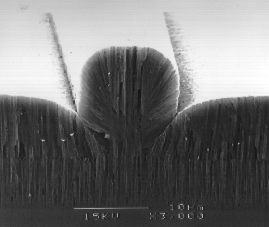
Fig.3: SEM cross-section of a BCW fabricated at 30eV
4. WAVEGUIDES CHARACTERISATION
The propagation losses of the BCW fabricated with 300 eV were found to be 1 dB/cm.
It is believed that the losses are predominatly due to structural defects in the
deposited material.
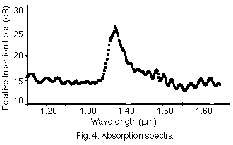
The absorption spectrum of the waveguide, using white light illumination and a spectrum
analyser, shows only one absorption peak at 1.38 m, due to O-H bonds, which does not interfere
with the propagation of the light at 1.3 m or 1.55 m; no absorption peak related
to N-H or Si-H absorption at 1.5 m was found. Such a peak is normally observed in PECVD deposited BCW, and is reduced only after
thermal annealing (1).
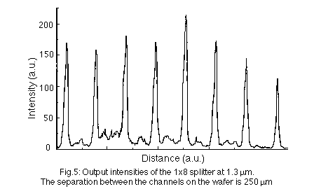
Using this technology, a 1x8 concatenation of Y-junctions has been fabricated.
The intensities on the 8 channels (at a wavelength of 1.3 µm) are plotted in
Fig.5. A photo of the splitter is shown on the previous web page.
5. CONCLUSION
By using the helicon plasma assisted processing of silica, we have been able to fabricate
BCW's at very low temperature. Never during the fabrication steps were the samples
submitted to temperature above 100 C. The losses of the Buried Channel Waveguides are still high (1 dB/cm), and it is
believed to be due to the microstructure of the material.
6. ACKNOLEDGMENTS
The project is supported by Ericsson Australia. The authors would like to thank TARL and RMIT.
7. REFERENCES
(1) C. H. Henry, R. F. Kazarinov, H. J. Lee, K. J. Orlowsky and L. E. Katz: 'Low-loss
Si3N4-SiO2 optical waveguides on Si', Applied optics.
, 1987, 26, (13), pp. 2621- 2624.
(2) G. Grand, J. P. Jadot, H. Denis, S. Valette, A. Fournier and A. M. Grouillet:
'Low-loss PECVD silica channel waveguides for optical communications', Electron. lett.
, 1990, 26, (25),pp.2135- 2137.
(3) Q. Lai, J. S. Gu, M. K. Smidt, J. Scmid and H. Melchior: ' Simple technology for
fabrication of low-loss silica waveguides', Electron. lett.
, 1992, 28, (11), pp. 1000- 1001.
(4) K. Imoto and A. Hori: 'High refractive index difference and low-loss optical waveguide
fabricated by low temperature process', Electron. lett.
, 1993, 29, (12), pp. 1123- 1124.
(5) E. S. Bulat, M. Tabasky, B. Tweed, C. Herrick, S. Hankin, N. J. Lewis, D. Oblas, and
T. Fitzgerald: 'Fabrication of waveguides using low-temperature plasma processing
techniques', J. Vac. Sci. Technol.
, 1993, A11, (4), 1268-1274.
(6) M. V. Bazylenko, M. Gross, P. M. Allen and P. L. Chu: 'Fabrication of low temperature
PECVD channel waveguides with significantly improved loss in the 1.50-1.55=B5m wavelength
range' to be published.
(7) G. Giroult-Matlakowski, C. Charles, A. Durandet, R. W. Boswell, S. Armand, H.
M. Persing, A. J. Perry, P. D. Lloyd, S. R. Hyde and D. Bogsanyi: 'Deposition of
silicon dioxide films using the helicon diffusion reactor for integrated optics applications', J. Vac. Sci. Technol.
A, 1994, A12, (5), pp. 2754-2761.
(8) A. Durandet and D. McKenzie: 'Effect of the energy of the ion bombardment on the
microstructure of PECVD SiO2' this conference.
(9) A. J. Perry, D. Vender and R. Boswell: 'The application of the helicon source
to plasma processing', J. Vac. Sci. Technol.
, 1991, B9, (2), pp. 310-316.
Optical Waveguide page |
SP3 home page